Company
Facilities
Vietnam Org Chart
Quality Certifications
Product & Services
PCB
PCBA
Capabilities
DFM Graphics
Technology Details
LeadTime
PCB Flowchart
PCBA Flowchart
Material
Contact
Toggle navigation
Company
Facilities
Vietnam Org Chart
Quality Certifications
Product & Services
PCB
PCBA
Capabilities
DFM Graphics
Technology Details
LeadTime
PCB Flowchart
PCBA Flowchart
Material
Contact
🔙 Back to DFM MAIN MENU
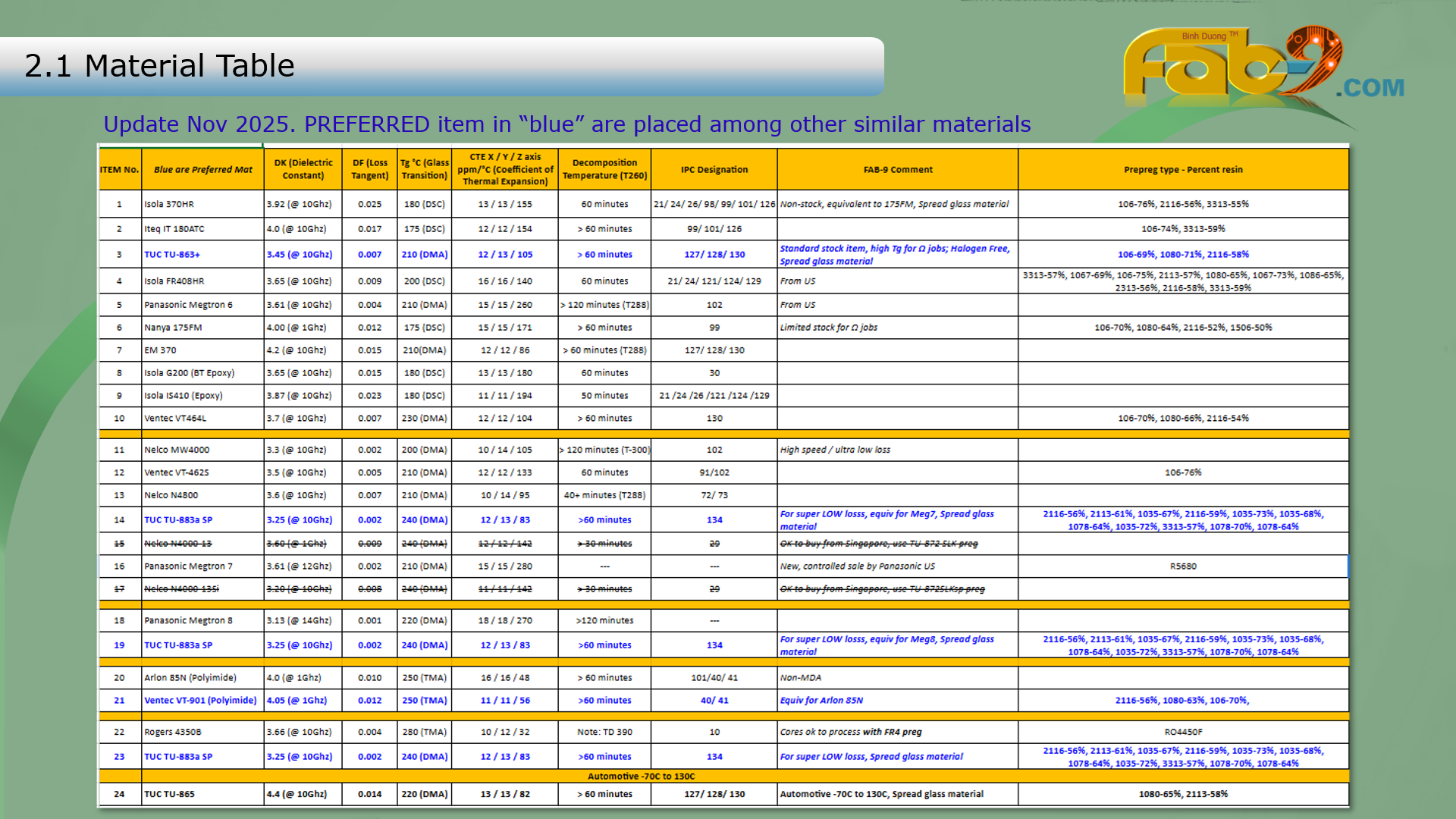
2.1 Material Table
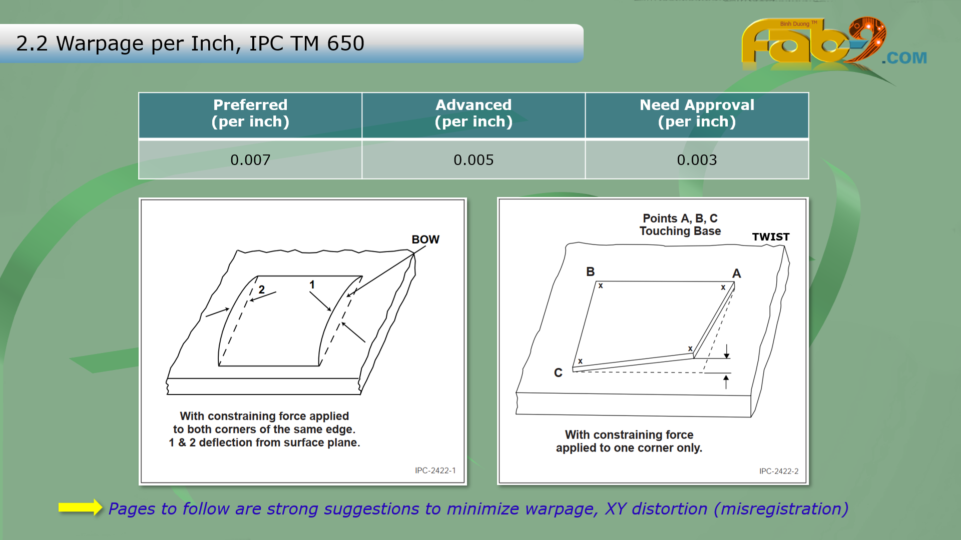
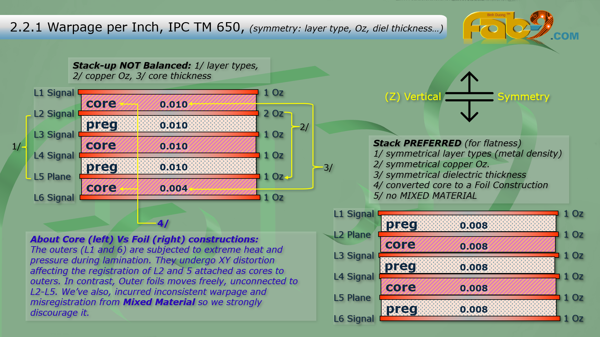
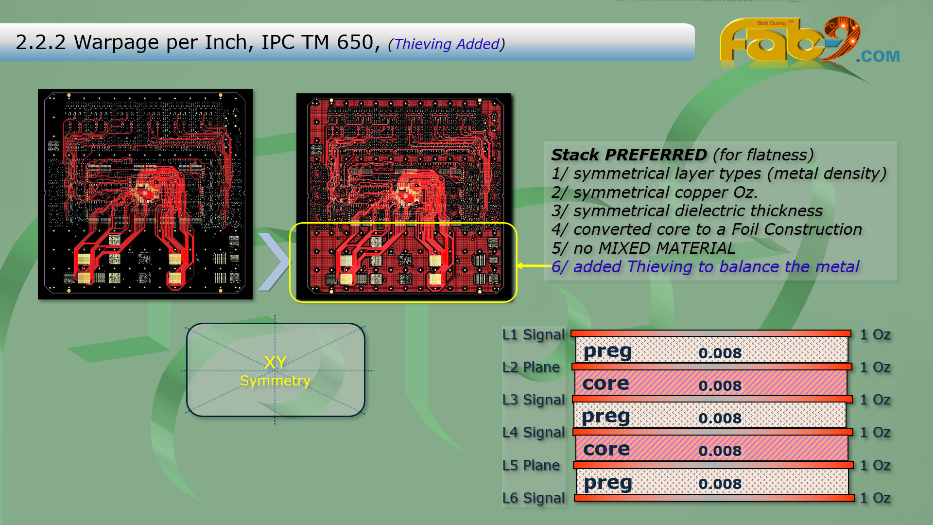
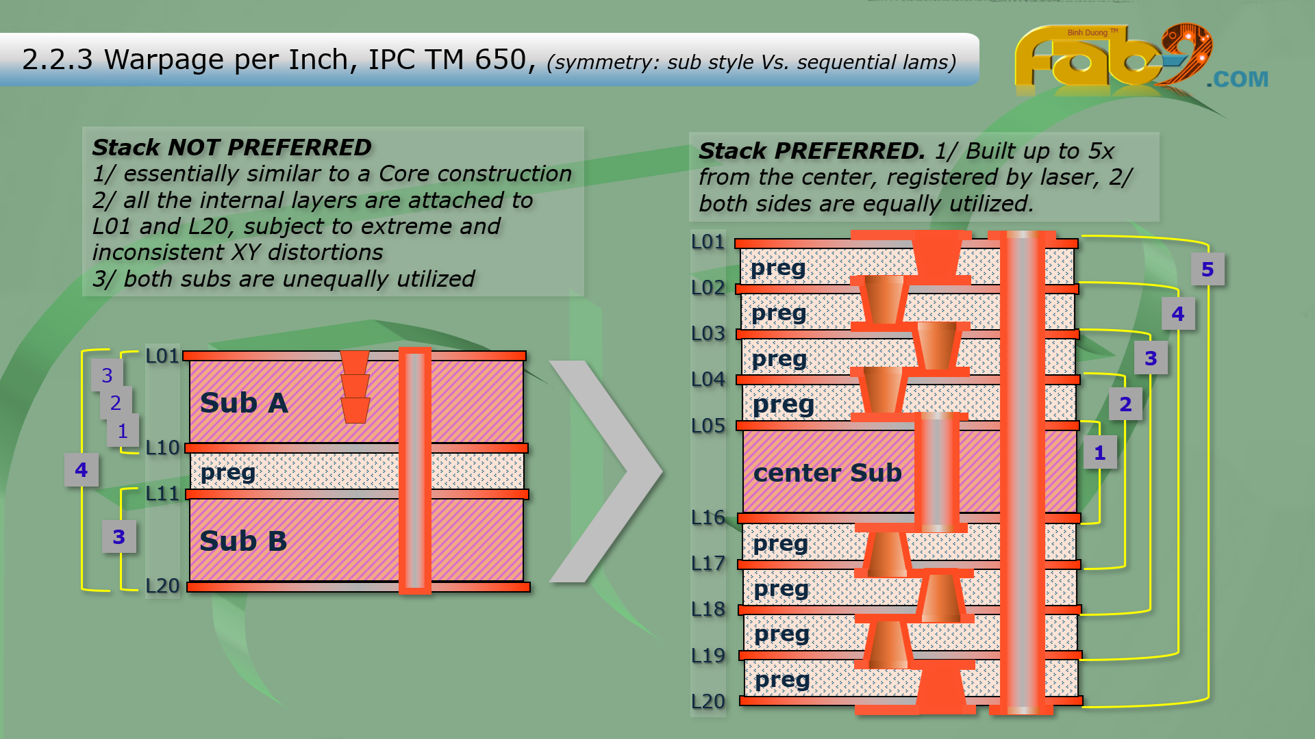
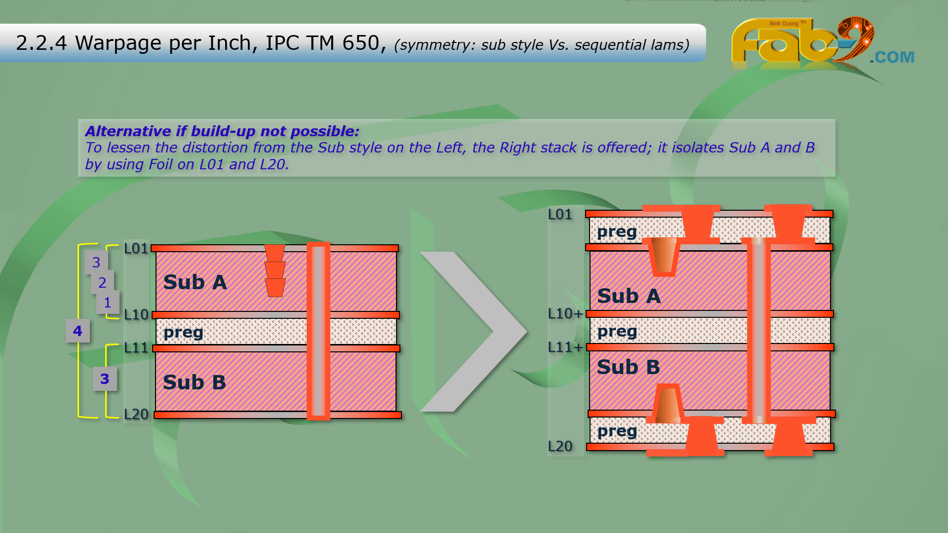
2.2 Warpage per Inch, IPC TM 650 (examples: 2.6.1 - 2.6.4)
2.3 Copper Foil Outer see 1.3
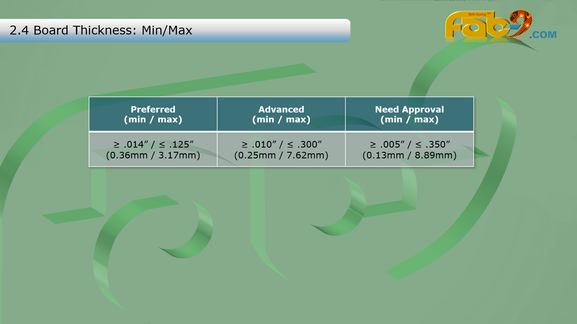
2.4 Board Thickness: Min/Max
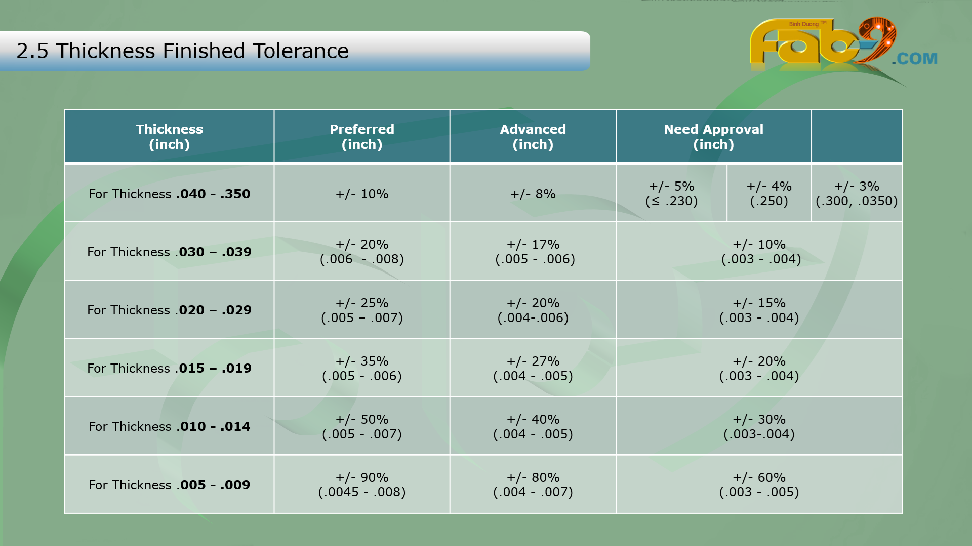
2.5 Thickness Finished Tolerance
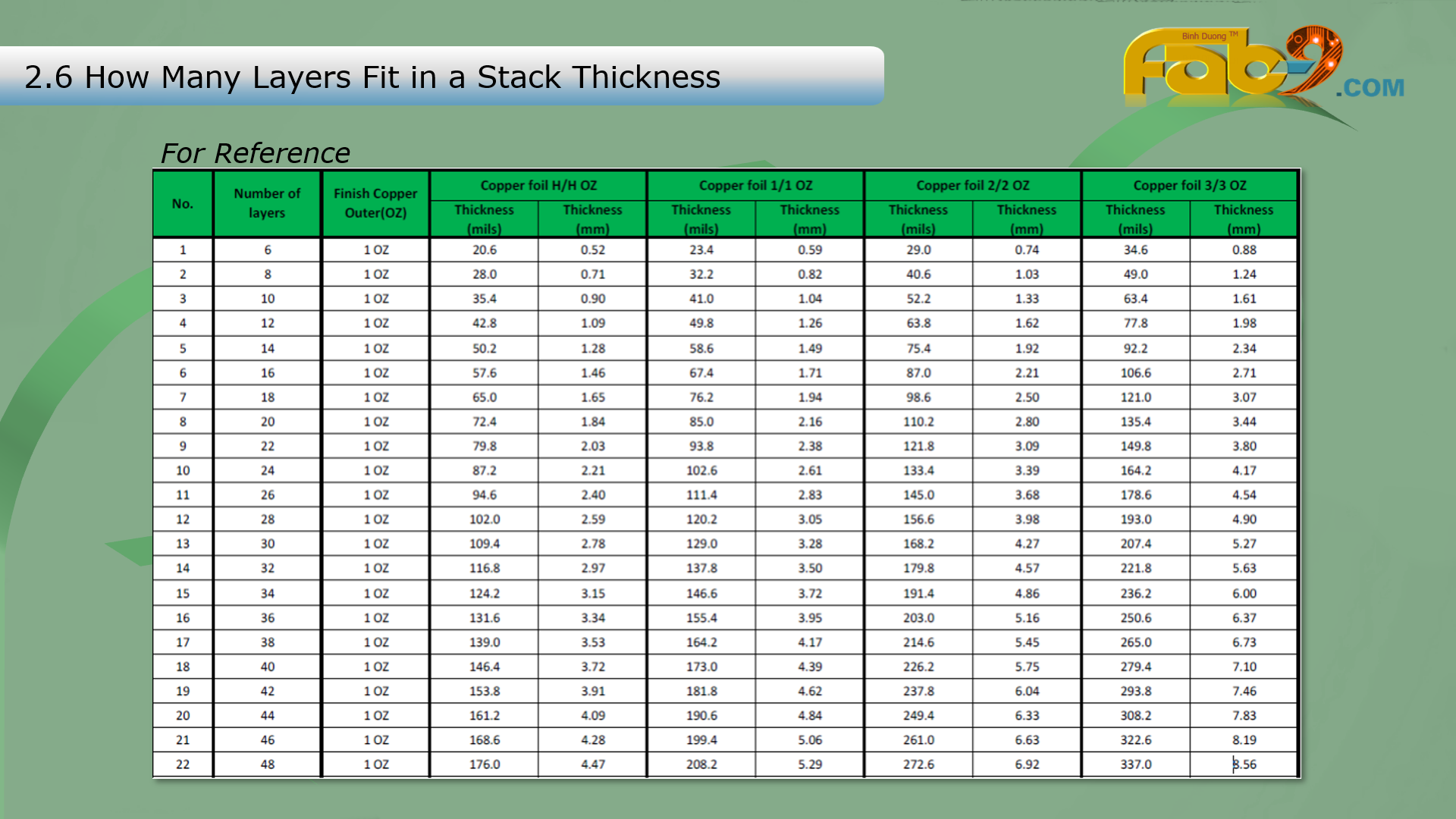
2.6 How Many Layers Fit in a Stack Thickness
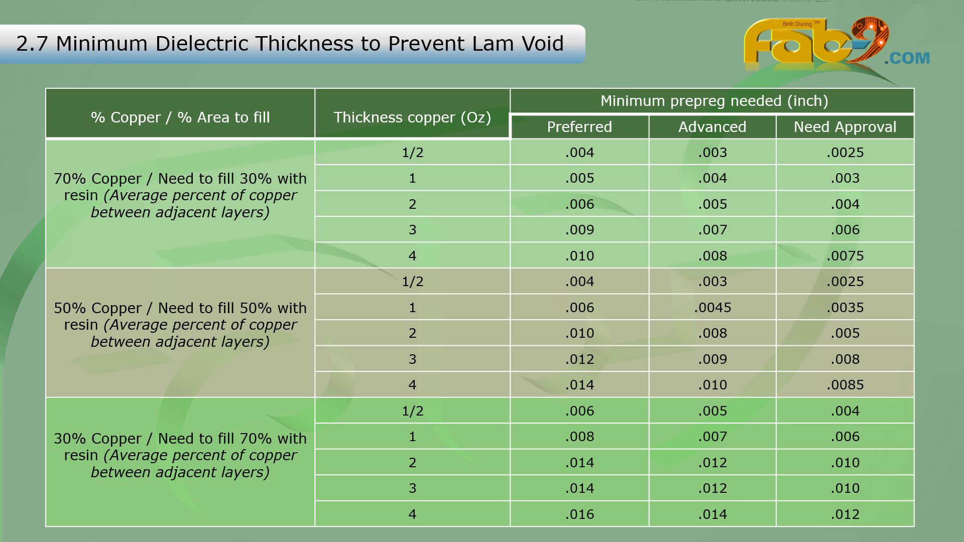
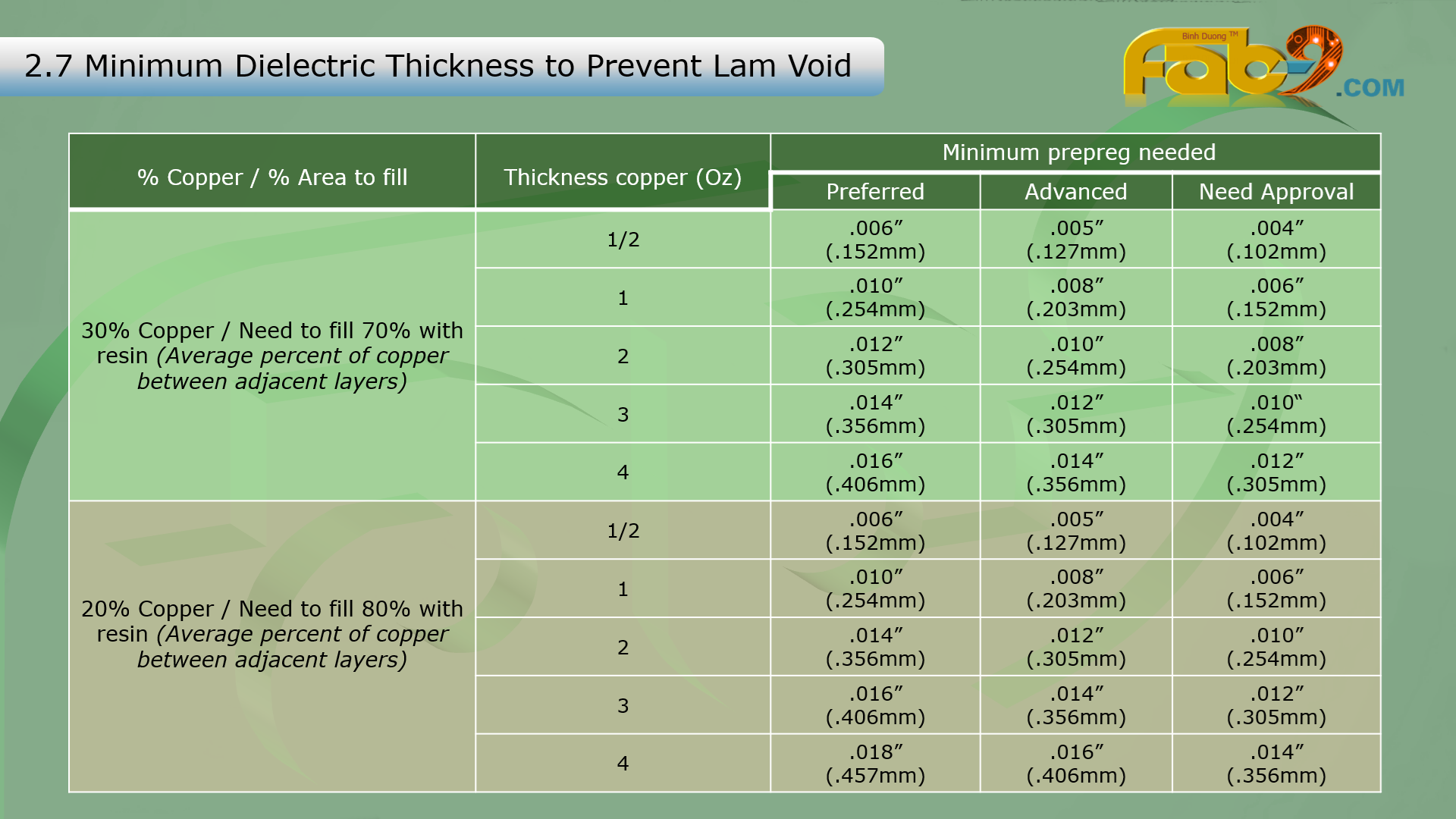
2.7 Minimum Dielectric Thickness to Prevent Lam Void
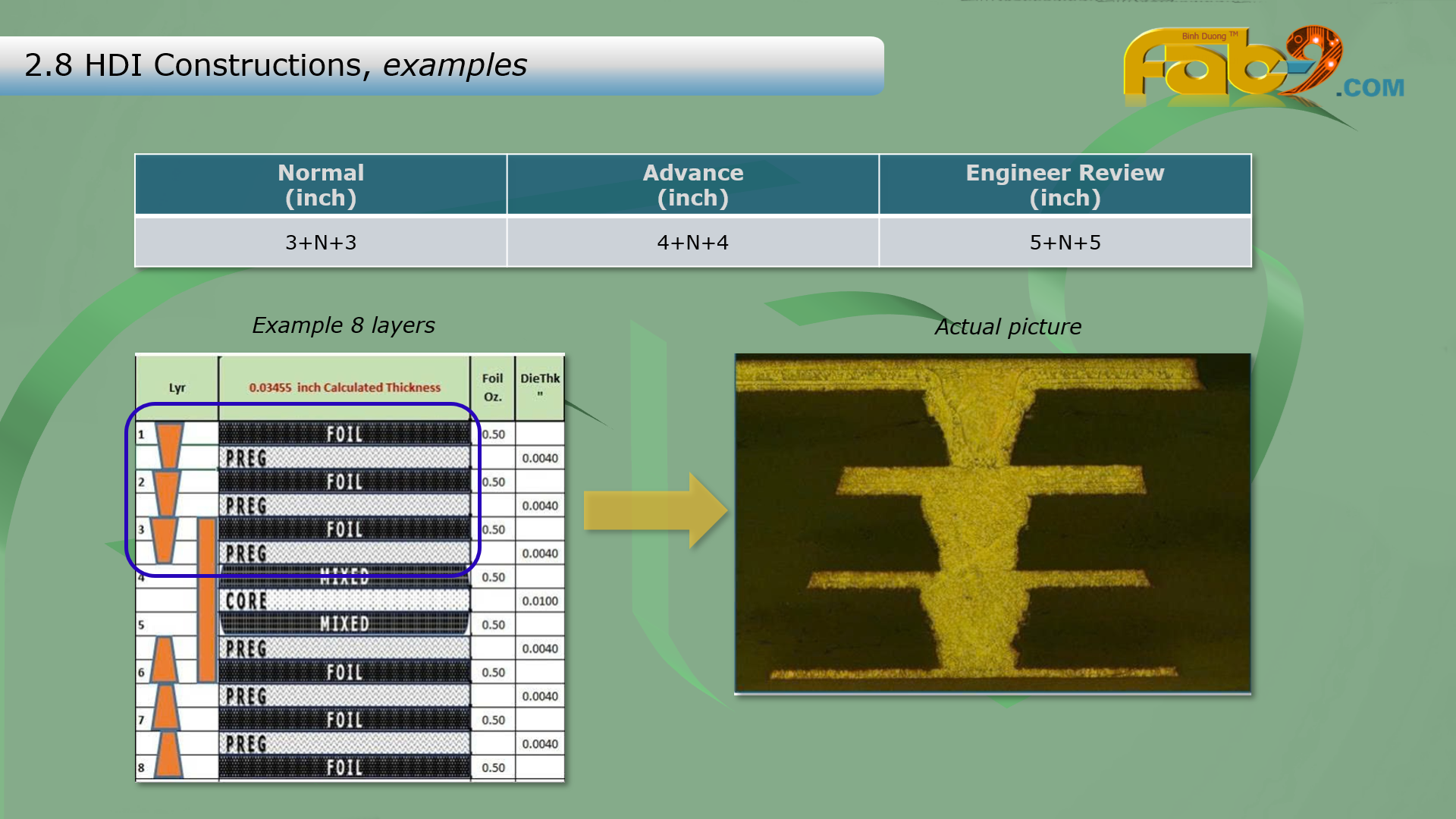
2.8 HDI Constructions, examples
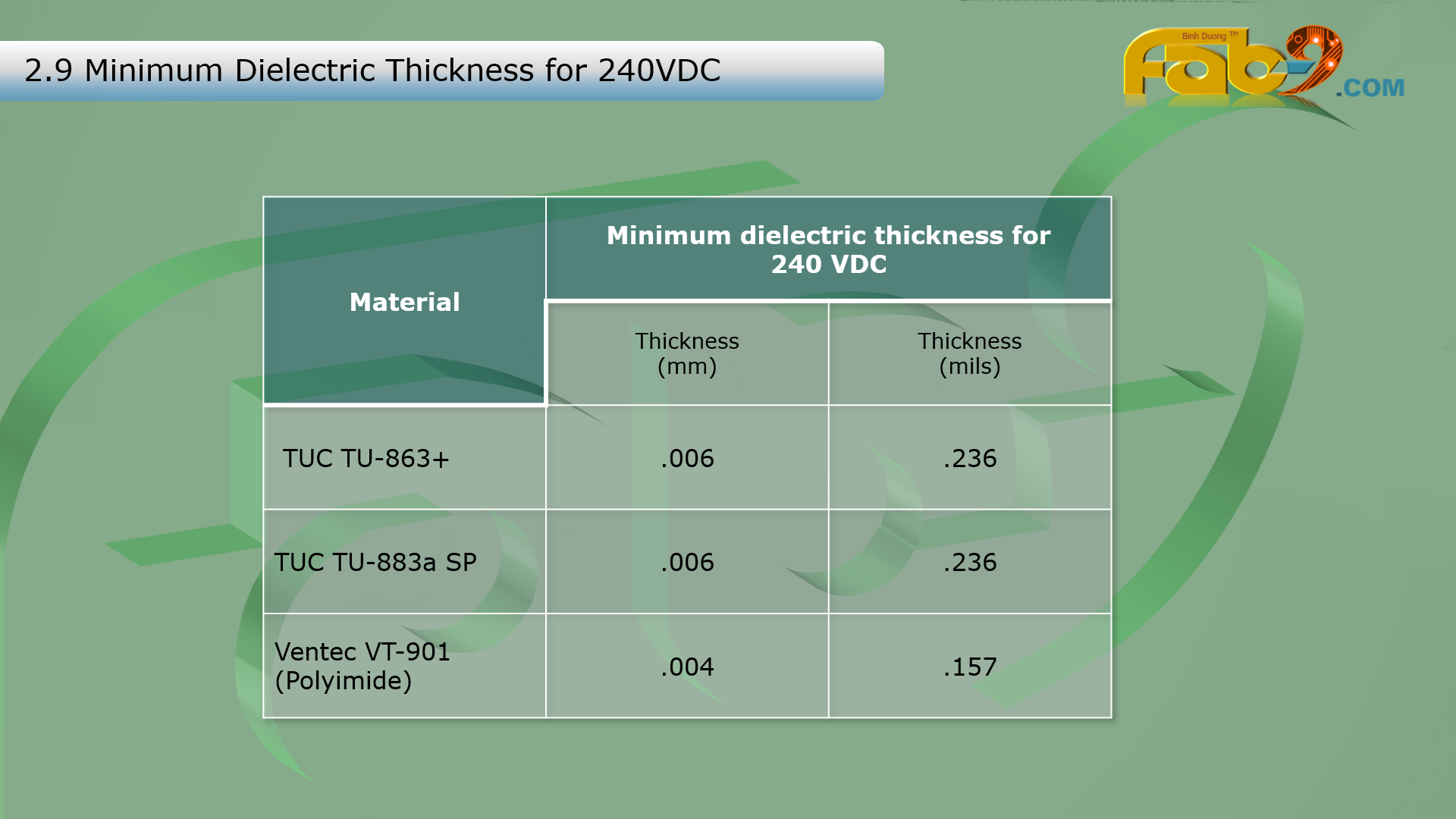
2.9 Minimum Dielectric Thickness for 240, 500 VDC